


Researchers at the University of Chicago Create “Quantum Highways” in a New Semiconductor
Creating advanced devices is a complicated process. Many times, quantum and advanced electronic devices require special materials, such as silicon semiconductors in order to work. This need has driven research in materials science, as investigators hope to find other useful components for these devices. One team from the University of Chicago has already found gold, or perhaps the material version of it, in their discovery of a new material called MnBi6Te10. In a new paper published in Nano Letters, the researchers outline the capabilities of this material, including its ability to create specific electron paths which can be helpful in improving semiconductors.
Describing a New Material
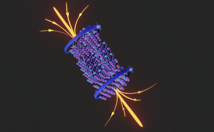
For a quantum computer to work, there needs to be a device used to connect qubits together and transmit their information, many times in the form of single electrons. previous research suggested that creating distinct paths through a material for electrons to move on would help to transmit this information. However, due to the freezing temperatures needed for many quantum computers to work, the types of materials that could be tested are limited. Because of this, the researchers at the University of Chicago turned to MnBi6Te10, which seemed to perform at better temperatures. “MnBi6Te10 is a layered quantum material,” explained lead researcher and Assistant Professor Shuolong Yang. “The best way to understand is to think about a Lego game or layered cheesecake. MnBi6Te10 is made of a stack of quasi-two-dimensional molecular sheets. There are two types of sheets: one MnBi2Te4 and another Bi2Te3. Each functional building block is comprised of one MnBi2Te4 layer and two Bi2Te3 layers.”
Due to its layering and composition, MnBi6Te10 has some unique magnetic and topological (an intrinsic property governing a material’s electronic properties) capabilities. This makes the material a perfect topological insulator, where the interior behaves as an electrical insulator but the surface acts like an electrical conductor. The contrast in these two areas allows for more control of where the electrons move in the material. “The Mn2+ ions in the MnBi2Te4 layer provide the strong magnetism,” added Yang. “Both the MnBi2Te4 and Bi2Te3 layers provide nontrivial topology. These two ingredients can create quantized edge conduction channels for electrons.” To test the properties of their new semiconductor, the researchers introduced magnetization using manganese (Mn). “Mn exists as Mn2+ ions in this compound,” stated Yang. “It provides a strong magnetization through a mechanism called ‘Hund’s rule.'” In Hund’s rule, individual electrons fill empty sections in the outer shells of an Mn2+ ion, and their spins (either spin down or spin up) all align to create units of atomic magnetization. “Among all the different elements, this is quite a high magnetization for a single ion,” Yang added.
Testing out a New Semiconductor at the University of Chicago
Imposing the magnetic field, Yang and his team were able to force the electrons to move in a single line on the material’s surface. This system gave the researchers an easier method to track the electrons. “We track the behaviors of electrons using a technique called Angle-Resolved Photo Emission Spectroscopy (ARPES),” said Yang. “This technique is is based on the famous theory by Einstein to explain this photoelectric effect. Essentially, we shine an ultraviolet laser at the MnBi6Te10 sample and kick out photoelectrons into a vacuum. We can experimentally measure the energies and momenta of these electrons, which allow us to understand their behaviors when they were still in the material. This technique reveals that electrons on MnBi6Te10 form a many-body quantum-mechanical state called a topological surface state. Moreover, this topological surface state is influenced by the strong magnetism, such that electrons like to flow with designated directions and spins.” Thanks to the technique, the researchers could induce “quantum highways” to study electron flow, controlling where the electrons moved.
With their experiment showing a new way to move electrons, the University of Chicago researchers are hopeful that MnBi6Te10 could be used in developing advanced devices like quantum computers. “This material exhibits all the essential physics for us to utilize the quantized conduction channel of electrons,” Yang said. ” Basically, when you think of classical computing devices, you need metal interconnects to connect different transistors. However, for topological quantum devices, the conduction channels need to maintain the quantum properties. The quantized channel of electrons in MnBi6Te10 fills this future technological gap. Of course, the research on the technological potential of this interesting material is still in its infancy. We are working on growing an ultrathin (< 10 nm) version of this material, as one step closer to making useful devices.”
Kenna Hughes-Castleberry is a staff writer at Inside Quantum Technology and the Science Communicator at JILA (a partnership between the University of Colorado Boulder and NIST). Her writing beats include deep tech, the metaverse, and quantum technology.