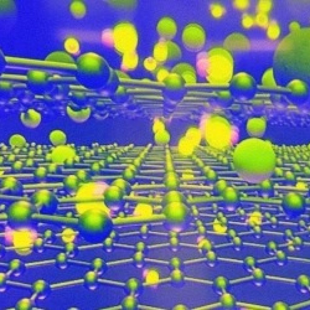
(ScienceDaily) Researchers may have cleared a significant hurdle on the path to quantum computing, demonstrating step-change improvements in the spin transport characteristics of nanoscale graphene-based electronic devices.
The team — comprising researchers from the National Graphene Institute (NGI) led by Dr Ivan Vera Marun, alongside collaborators from Japan and including students internationally funded by Ecuador and Mexico — used monolayer graphene encapsulated by another 2D material (hexagonal boron nitride) in a so-called van der Waals heterostructure with one-dimensional contacts. This architecture was observed to deliver an extremely high-quality graphene channel, reducing the interference or electronic ‘doping’ by traditional 2D tunnel contacts.
‘Spintronic’ devices, as they are known, may offer higher energy efficiency and lower dissipation compared to conventional electronics, which rely on charge currents. In principle, phones and tablets operating with spin-based transistors and memories could be greatly improved in speed and storage capacity, exceeding Moore’s Law.
Lead author of the study Victor Guarochico said: “Our work is a contribution to the field of graphene spintronics. We have achieved the largest carrier mobility yet regarding spintronic devices based on graphene. Moreover, the spin information is conserved over distances comparable with the best reported in the literature. These aspects open up the possibility to explore logic architectures using lateral spintronic elements where long-distance spin transport is needed.”
Graphene spintronics: 1D contacts improving mobility in nano-scale devices may clear hurdle on path to quantum computing